Freshwater Crocodile

Competition Pro Mini refurbishment

I recently got two Competition Pro Mini joysticks. The full-size Competition Pro was probably one of the most famous joysticks back in the 1980s and early 1990s. This model was said to be unbreakable, and was able to withstand even long and intensive gaming sessions. If one of the microswitches eventually failed, it was easy to get a new one from an electronics store and replace it just by using a screwdriver, no soldering required.

The Mini models came to the market in 1992, and were by far not that robust. My two examples had broken microswitches at the left direction. The microswitches are soldered to the PCB, and they are also out of production.

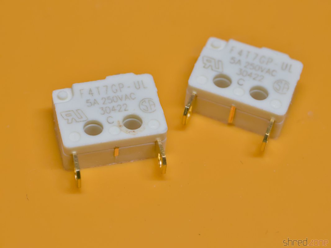
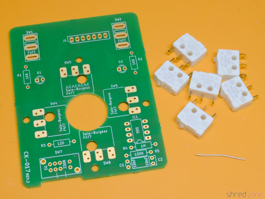
The closest available replacement is the Saia-Burgess F4T7UL and F4T7GPUL (the latter one with gold-plated contacts). Unfortunately it has different solder tails, so it cannot be used as a drop-in replacment.

Left: The original microswitch. Right: The Saia-Burgess F4T7GPUL, with shorter solder tails.

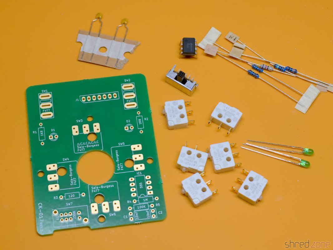
I decided to build up a completely new PCB by InsaneDruid instead. It is a replica board with exactly the same size and fuctionality, but it is prepared to use the Saia-Burgess switches.

Auto-fire Model

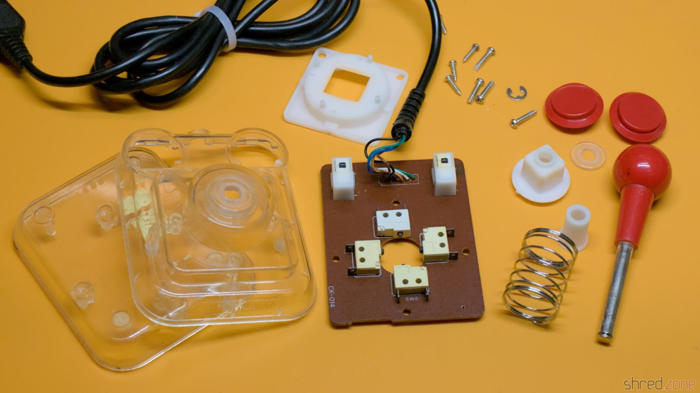
The first thing I did was to completely disassemble the joystick. All plastic parts were cleaned in an ultrasonic bath. Meanwhile I noted the color order of the wires before cutting the cable from the old board.

The individual parts of the joystick.

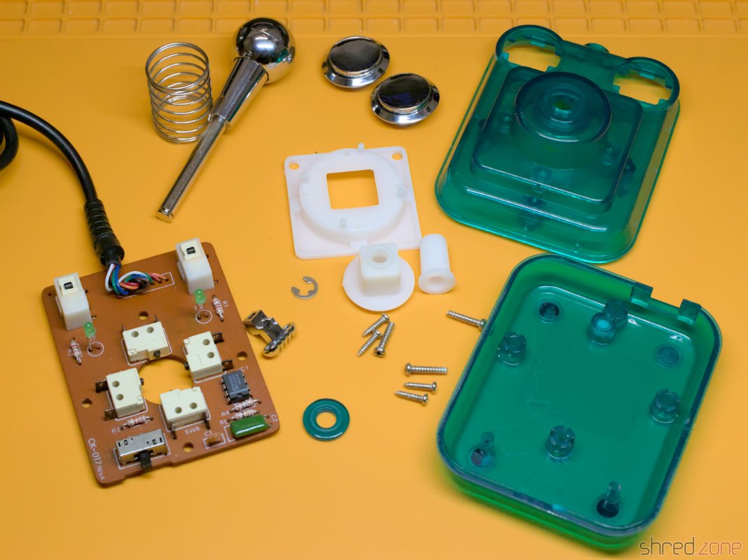
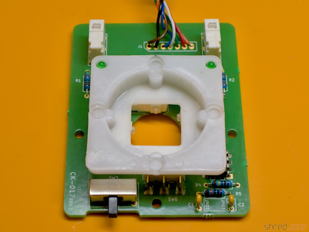
The new board only needs very few components. Except of the switches, all of them are standard ones that can be found in any electronic store. The switches can be found at distributors like Mouser.

The replica PCB and all required components.

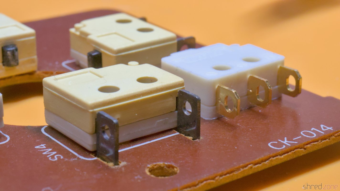
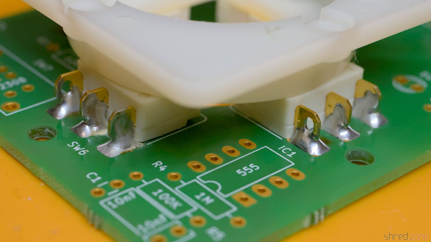
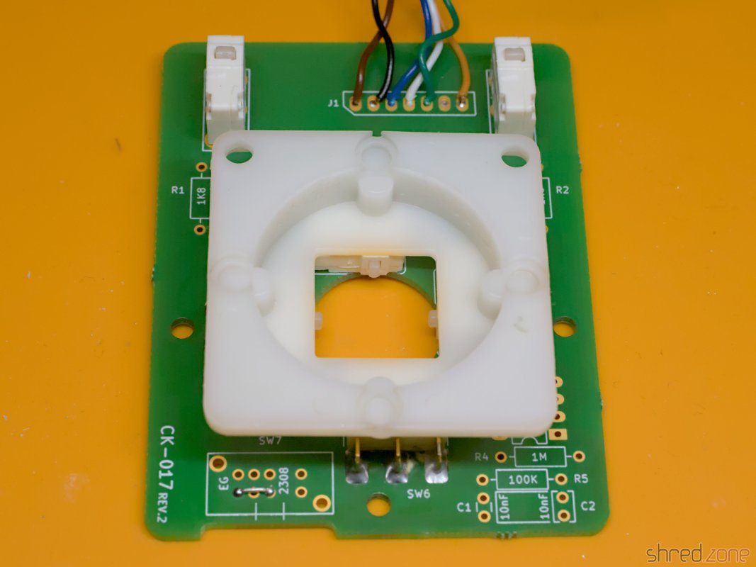
For the four directions, I first mounted the microswitches to the holder frame. This way it will be easier to perfectly align the switches to the PCB.

For the fire buttons, the middle solder tail needs to be cut off. Otherwise it will collide with a peg of the bottom case shell later.

The four directional switches are mounted to the frame using the four shorter original screws. Check the correct position of the plungers, and make sure the switches are lying flush to the frame. For the two fire buttons, the middle solder tails need to be cut off. It would collide with a peg of the bottom shell.

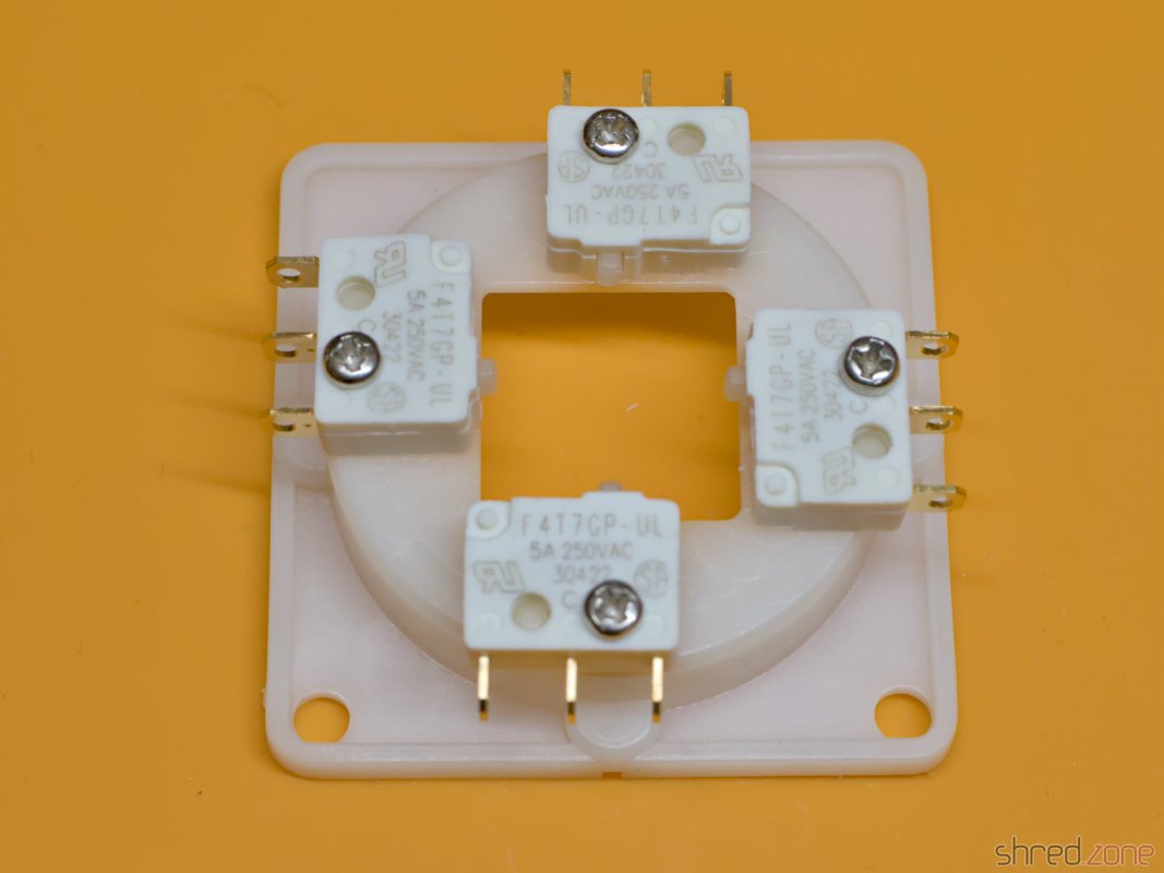
Usually we would start with the flattest component, but in this case, I recommend to start with the four direction switches. Position them to the frame so the four screws are perfectly aligned with the corresponding PCB holes. Make sure that the two LED holes are aligned to the "up" direction. Then start soldering the switches to the PCB, using a generous amount of solder.

Additionally you can use wire brackets to secure the switches using the provided mounting holes. I was too lazy to do that though.

The four switches are soldered to the upper side of the PCB. You can use wire brackets for additional securing. The bottom side, with the four screw heads centered in their PCB holes.

The remaining components are just soldered to the board. Finally the original cable is wired to the board, with the original order of wire colors.

The completed joystick board.

After that, the joystick is ready for reassembly.

Standard Model

My other joystick is a standard model without auto-fire function. Again, I disassembled it. All plastic parts were cleaned, while I noted down the color order of the wires.

The standard model, disassembled (before cleaning).

The cable of this model does not provide a +5V supply. For this reason, there is no need to populate the components for the auto-fire. We can also save the LEDs, as they won't light up.

The standard model needs considerably less components: Just six switches, and a short piece of wire.

The preparation is the same as for the other joystick. The four direction switches are mounted to the frame, and the two fire switches lose their middle solder tail. After that, the frame with the switches is aligned and soldered to the board, followed by the fire switches.

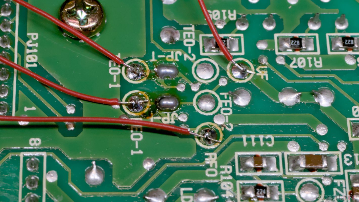
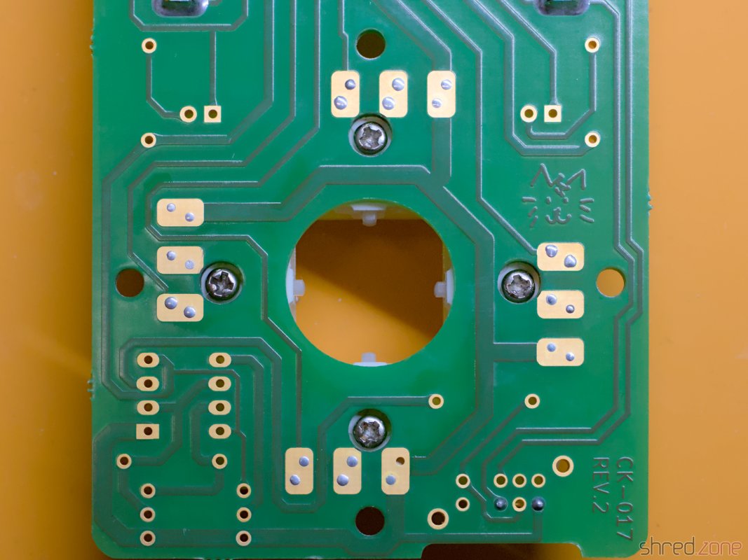
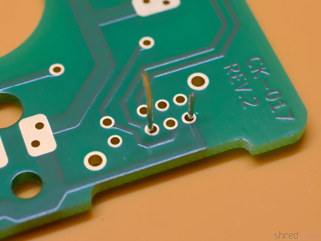
We do not need to populate the mode switch. However, we need to solder in a wire bridge to pins 5 and 7 (see photo), otherwise the fire buttons won't work at all.

Bridge pins 5 and 7 with the wire.

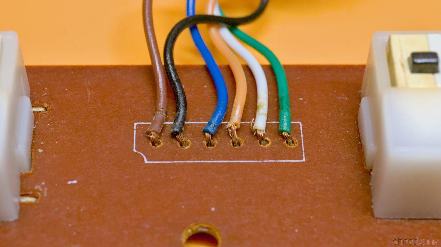
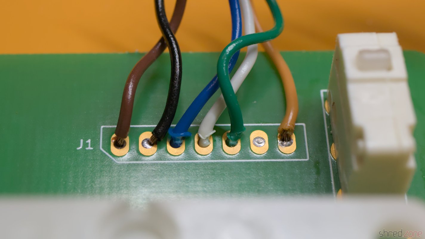
The wires need a different order. On the original board, the "fire" signal is at the third position from the right (the orange wire on my joystick). On the new board, that signal is on the very right pad. The one left from it stays empty. For the remaining wires, the original order can be kept.

The original wiring. Your colors may be different. The wiring of the new board, with the orange wire to the right.

After that, this board is completed as well, and the joystick can be reassembled.

The completed standard joystick board.

The joysticks look as good as new now, with their clean case and their brand new boards.

The refurbished transparent green and transparent white Competition Pro Minis.

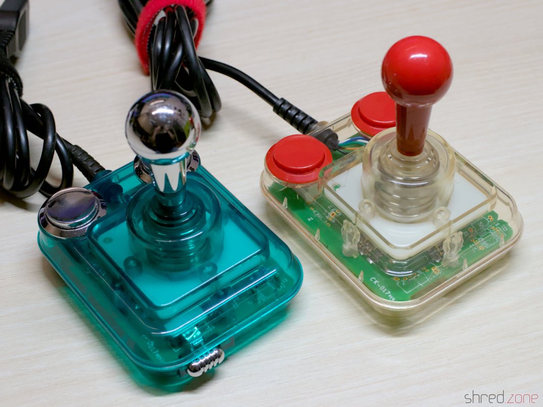
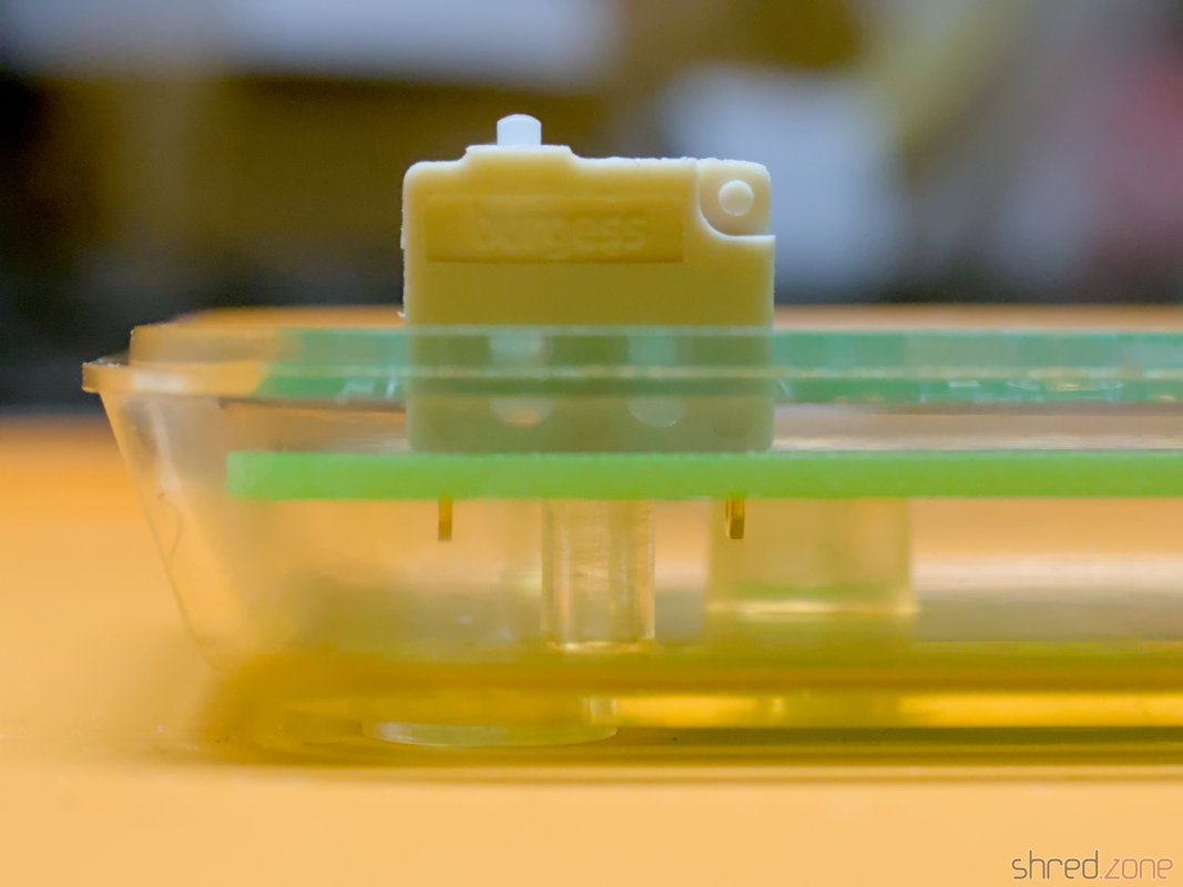
The ENIG plated PCBs are a true eye-catcher in their transparent cases.

Goodbye Blue Bird

After being on Twitter for 13 years, I decided that it is time to leave the platform for good. They say you should always leave on a high note. Maybe I have missed that moment already.

Today I have closed my account there. My handle was shred_ (with a trailing underscore).

You can follow me in the Fediverse: @shred@oldbytes.space

Thank you, blue bird! I have learned a lot from you and met a lot of great and interesting people. It was fun while it lasted.

PS: I have no plans to join other social media platforms. No need to send me invite codes. 😉

CD32 Refurbishment, Part 2

In the first part I successfully repaired an Amiga CD32 that got broken due to leaking capacitors and a botched restauration attempt. In this part I replace the laser pickup and calibrate the CD drive.

The old laser pickup of the CD32 might be worn out due to age and use. A common symptom is that the CD32 is unable to play CD-R media, or it is only capable of playing music CDs. There is no way to make the CD32 accept CD-RW media though, since they use a dye instead of pits that reflect too little light.

But before we start, read this:

CAUTION: The laser pickup is very sensitive to ESD. Use protective measures (such as an antistatic wrist band).

Make sure that the laser is always covered when the machine is turned on. Do not look into the laser beam.

I should also mention that I am not a trained technician. I have read manuals about how to calibrate CD drives, and it has worked for me. However, I don't claim that this is the best or most professional way to do a calibration.

You will need a soldering iron for the pickup replacement, and you will definitely need a scope for calibration. The drive might work without calibration after replacing the pickup, but the result will not be optimal.

Pickup Replacement

I started with disassembling the CD drive. I removed it from the case. Then I carefully disconnected the pickup and the motor unit, and removed the four screws that hold the pickup frame. There is a metal shield covering the pickup that needs to be removed as well.

The frame with the laser pickup, spindle motor, and tracking mechanics.

The laser pickup unit is a Sony KSS210A. It is long out of production, but replicas are sold at online marketplaces for a few bucks. To remove the old pickup, I first removed the white cog wheel, then I pulled out the metal rod (it is secured by a plastic clip that can be pushed to the side). Since I was on it, I cleaned the old grease from rod and the cog wheels, and applied a bit of fresh silicone grease. After that, I mounted the new pickup and reassembled the CD drive just in the opposite order of disassembly.

After the new pickup unit has been connected to the controller, a solder blob on the pickup unit must be removed! It protects the laser from ESD, but will damage the drive controller if it is still there when powering on the drive.

Closeup of the pickup module, with the solder blob on the top right.

If you want to keep the old pickup module as a backup, you can also apply a solder blob there before disconnecting it.

Preparation

For calibration, I opened the metal shield of the drive controller, and found a surprise underneath. There was a tiny board glued to the main PCB, and connected to some points with seven wires:

A tiny modification board is glued and connected to the PCB.

I first thought this could be some kind of mod to circumvent copy protection measures, but then again, the CD32 does not have a sophisticated copy protection scheme. Later I found the answer in a YouTube video: This modification immediately cuts the power from the laser and the spindle motor when the lid of the CD drive is opened. I could find many photos of the controller board without the modification, so I guess that it was a product safety requirement for selling the CD32 on the German or European market.

Okay, let's get back to the calibration. As a preparation, I first soldered wires to the VF, RFO, TEO-1, and FEO-1 test points. I recommend to use wires of different colors, it makes the calibration much easier. Unfortunately I only had red wire at hand, so I had to check each time which wire went where.

Wires are soldered to the VF, RFO, TEO-1, and FEO-1 test points.

After that, I noted down the current settings of the four pots on the controller board, and of the pot on the laser module, using an ohmmeter. If I should mess up the calibration for some reason, I could always go back to these settings. (A photo of the pot positions is not sufficient, as very tiny changes can already make a huge difference.)

The four pots for calibration are on the side of the controller. See the silkscreen for which pot does what.

For the calibration, the drive needs to be connected to the mainboard again. The case top (with the LEDs, reset button etc) needs to be connected as well, since the CD32 won't attempt to read the CD unless the drive lid is closed. The laser pickup is moving during operation, and should have sufficient room for that.

To fix the CD to the spindle, I removed the spindle clamp from the inside of the lid, and used a bit of tape to keep the loose part fixed in the center of it. It is held to the spindle with a magnet, and ensures that the CD won't slip on the spindle.

Calibration

The calibration process is explained in this blog article by TSB. My attempts to explain it would be far worse. 😉

However, it turned out that on my drive, the process didn't work like that. After doing the first steps of the calibration, my drive was suddenly unable to spin up the CD for reading. I was lucky that I noted the pot positions (like recommended above), so I could revert to the original settings and start anew.

Then I first calibrated the TEB pot until there was approximately 0 mV between TEO-1 and VF. The drive was still working after that. However, after I calibrated FEB like documented, the drive stopped working, so I reverted that change again and moved on with calibrating the laser power.

CAUTION: Be very careful with the pot on the laser module and only turn it in very small increments. Otherwise the laser may be permanently damaged.

There is a drop of varnish on the pot from production that may require some force to break, so it might be a good idea to first turn the pot while the device is powered off, and then use an ohmmeter to return it to the factory setting that you previously noted.

To calibrate the laser power, I connected my scope to RFO and ground. Then I put a music CD on the spindle and started playing track 1. The scope should now show a so-called "eye pattern":

The tricky part is to turn the pot on the pickup module carefully while the CD is playing. I turned it very carefully until I reached a peak-to-peak voltage of about 900 mV. Take care never to exceed 1200 mV!

After that, I adjusted the FEB pot on the controller board until I reached a maximum amplitude on the eye pattern.

The last two pots, FEG and TEG, are calibrated by scoping the FEO-1 and TEO-1 test points against ground, respectively. The drive should play track 1 of an audio CD and should be in pause mode while calibrating.

I tried to find the sweet spot where the signal on the scope was as smooth as possible, and the correction noise from the optics was as silent as possible. There is a trade-off between these goals, and I found that the best results came from listening to the pickup noise and using my intuition.

The calibration is complete after that, and the CD32 can be assembled again.

One final tip: burn CD-Rs for your CD32 at the lowest speed supported by your recorder. This will increase the contrast of the data on the CD. Also, prefer CD-Rs that are not transparent when held up to the light.

CD32 Refurbishment, Part 1

An Amiga CD³² Game Console in good condition. I found this CD32 for a fair price, and bought it. The optical condition of the case is quite okay. It has some visible scratchmarks. The previous owner tried to fix them, but made it even worse. At that time, I wasn't aware yet that this would be the main theme of the whole restauration.

Together with the console, I got a PSU and an edutainment CD for learning math. The PSU wasn't the original one, but a simple power brick with a CD32 connector soldered on. The gamepad was missing, unfortunately, but I found a Honey Bee joypad as replacement a bit later.

Let's have a look inside the machine.

The State

The seller sold it as broken because it showed no picture. When I opened the case, the machine told me a completely different story. There was an attempt to recap the machine. It was abandoned after replacing the TH and the 100µF SMD caps, probably because the picture was gone after that.

I also found blotches of green varnish, presumably simple nail varnish. It was under the replaced SMD caps, but also on solder joints and some vias. The varnish made no sense at all, except of maybe cosmetical reasons.

And I found this:

Closeup of a Sony CXA1145 Video Encoder chip. The first pin is cut off, and the PCB underneath is damaged.

I assume that when the picture was gone, the guy who tried the refurbishment assumed that the video encoder chip got damaged, but had no equipment at hand to unsolder an SMD chip, and attempted to cut it from the board pin by pin instead.

I found no further traces of mistreatment of the poor board. It's going to be enough of work to fix the current mess already.

To be honest, I am pretty upset about that. There is a difference between if the machine shows no picture after decades of storage, or because of a botched refurbishment attempt. The seller should have pointed out that fact.

Fixing the Mainboard

First I attempted to restore the picture by replacing the obviously broken video encoder chip. I also replaced an electrolyic cap next to it that looked suspicious. Unfortunately that did not bring back the video signal.

The question was now whether I was getting no picture because of further errors in the video area, or because the machine is not starting at all. To find out, I inserted a DiagROM and connected the CD32 to my PC. The DiagROM started and logged no errors to the console. So the good news was that the machine is basically working.

I then decided to remove everything from the previous restauration attempt, so I could start anew with a known state of the mainboard. I removed all the electrolytic caps, even those that had already been replaced, and cleaned off the green varnish with acetone and IPA.

There was a strange solder blob on the bottom side, covered with a layer of varnish. When I tried to clean it up, I smelled that revealing fishy smell of old electrolyte. I generously removed the SMD parts on both sides in that area, cleaned the board and checked the tracks and vias.

The bottom side of the audio area, as I found it. There is a strange solder blob covered in varnish. I generously removed all components around the affected area, and cleaned it. Fresh components soldered in. A track was damaged and needed to be fixed with a wire.

Unfortunately, I ripped off a few pads on the 100µF capacitors while doing so. I guess the leaked electrolyte and the thermal stress of two recappings was just too much for them.

Then I soldered in new components in that area, and fixed the broken pads with bodge wire. For two SMD capacitors, the board offered an alternative use of TH caps, which I thankfully accepted. The area is now looking quite ugly, but at least it should work again.

The top side of the audio area after removing the SMD caps. Two 100µF caps lost a pad due to thermal and mechanical stress. The same area, with fresh SMD components. Two of the SMD caps are replaced with TH ones. A broken track is fixed with a wire.

When I checked the tracks and vias at the other 100µF SMD caps, I found broken connections at C236 and C237. They are used for the luma or composite video signal, so the broken connections caused a black image.

The connection between the left pad and the via was broken, presumably while scraping off the solder mask. The only way was to fix it with a piece of wire. The connection between pin 20 and the right pad of C237 was broken as well, and disconnected the composite signal from the outputs.

I also found a broken via near C409, which carries the CSYNC signal. The missing connection causes a missing video sync signal at the outputs. I fixed it by opening the via and exposing the connected tracks on both sides, then soldering a thin wire to the tracks.

The broken via, before I fixed it with wire.

So there were more than enough reasons for this board to show no video picture.

The TH capacitors on the board are a bit special. For C408 and C811, the silk screen shows the positive end at the wrong side. Even Commodore soldered in the capacitors in the wrong orientation, and you will find many CD32 out there with bloated caps at that position. I decided to solder in SMD caps there instead, which can be soldered in like shown on the silkscreen.

After that, I checked the machine, and to my amazement, it was working again:

So the mainboard was repaired and refurbished. I checked all the video and audio connectors, and found a signal everywhere. The machine was also running stable.

The refurbished mainboard.

I'm glad that the machine turned out to be repairable.

In the next part, I will replace the laser module and calibrate the CD drive.

Building a ZX Dandanator Mini

The ZX Dandanator Mini in its printed case. The main way to load software into the ZX Spectrum was via audio tapes. There have been floppy drive extensions and Sinclair's proprietary Microdrive solution, but audio tapes were cheap and ubiquitous, and cassette recorders could be found in virtually every household.

The downside was that it was uncomfortable. Tapes are slow. It took several minutes to load a game into the machine. If you had a "collection" of multiple games on one tape, you first had to wind it to the correct position. When I got my first Amiga with floppy drive, I never really looked back to those times when I had to use audio tapes.

Today I own a couple of ZX Spectrums, but I don't have a tape recorder anymore. To load software into the machine, I usually use my PC's headphone jack and tzxplay. But there is a more elegant way. The ZX Dandanator Mini by Dandare is an extension with 512KB of Flash memory where you can store your most favorite games. A boot menu permits to select one of these games, which is instantly loaded into memory. It also provides a Kempston compatible joystick port.

When I started to build my ZX Dandanator Mini, I found that the documentation of the project left a few questions open. I hope my comprehensive blog article will help others to build their own one.

Parts

It only needs a few components. Fortunately, the Dandanator's bill of materials is quite short, and all the components are easy to find, maybe except of the edge connector.

  • 1x GAL 22V10 (+ DIP20 socket)
  • 1x PIC 16F1826-I/P (+ DIP18 socket)
  • 1x SST 39SF040 Flash ROM (+ PLCC32 socket)
  • 1x 1N4148 (TH)
  • 2x 10kΩ resistors (TH)
  • 5x 100nF ceramic capacitors (TH)
  • 1x D-Sub connector, 9-pin male, right angle, Europe style (e.g. this one)
  • 2x pin headers, 2-pin
  • 1x jumper
  • 2x 6 mm tactile switches (17 mm tall if you use the 3D printed case)
  • 1x PCB (Gerber files are here)
  • 1x ZX Spectrum edge connector (can be found in retro shops, online marketplaces, or just DIY)
  • 1x 3D printed case (optional)

You will need a programmer that is able to flash the PIC, GAL, and Flash ROM (e.g. XGecu TL-866II Plus with PLCC32 adapter). I also recommend a good PLCC chip puller.

Classic GALs are out of production, but can still be found as NOS parts in online marketplaces. A replacement that is still produced is the Atmel ATF22V10C-10PU. If you use that one, you will also need a 3.3kΩ 6-pin bussed resistor array. More about that below.

Assembly

The assembly is straightforward. You start with the flattest components and work your way up to the tallest. There are no SMD components, so even a soldering novice should have no problem.

Make sure the sockets are oriented correctly. Unfortunately there are no marks for pin 1 of both DIP sockets on the silkscreen. They should be oriented with the notches near the buttons, like seen on my photo. The PLCC socket should match the outline on the silkscreen.

There is no pin 1 marker for the orientation of the DIP sockets on the silkscreen. The notches are on the side of the switches.

The edge connector is usually meant to be soldered upright, not to the edge of the PCB, so you first need to bend the pins to the inside. If done correctly, the edge connector should sit centered, and all pins should touch the pads of the PCB. Also make sure to solder the connector to the correct side of the PCB, which is the one with the short pads. The connector on the other side is meant for further expansions, like a joystick interface, but you can even stack multiple Dandanators together.

If you intend to use the 3D printed case, leave a gap of about 2 mm between the PCB edge and the connector.

Make sure to solder the edge connector to the right edge. 😉

Some of the pads are close to the edge connector on the back. It's easy to spill some drops of solder on the pads while soldering. A bit of Kapton tape is a good way to protect them.

There is not much space between the vias and the pads of the edge connector.

A problem with the ATF22V10C is that it does not provide internal pull-ups at the inputs. This means that if no joystick is connected, the inputs are floating, which could lead to problems. On my system, if no joystick was connected, the first game on the list was always started immediately. A possible solution is to solder a bussed resistor array to the bottom side. The resistors are connected to pin 8, 9, 10, 11, and 13 of the ATF22V10C. The common bus is connected to pin 24. Take care not to connect or short circuit adjacent pins.

This problem should not arise with the ATF22V10B, but at the time of writing, this variant was either out of stock or ridiculously expensive.

I soldered a resistor array to the ATF22V10C. It's a 10 pin one with the unused pins cut off because I had no smaller one at hand.

While this issue likely won't occur with older GALs, the manufacturers still recommend not to let input pins open. In my oppinion, the pull-up resistors should have been a part of the Dandanator design.

The Dandanator, fully assembled. Do not bridge the "Serial Pins" (as opposed to what can be seen here).

In a final step, clean the board and inspect it for solder bridges and other errors. A short circuit can damage the power converter inside the ZX Spectrum, which is a bit difficult to repair.

The "Joystick" header is for enabling the joystick port, and should be bridged unless you plan to use another joystick interface. The "Serial Pins" header seems to be there for in-circuit programming, and should not be bridged. (It won't cause any damage if you accidentally bridge it, but it will be like permanently pushing the joystick to the right.)

When the assembly is done, the next step is to program the chips. They all are programmed differently.

Flashing the Chips

  • GAL: The fusemap can be downloaded here. If you use an ATF22V10 and the XGecu programmer, make sure to select the (UES) variant as chip type.
  • PIC: An initial firmware can be downloaded here. I have tried to flash it with the minipro software, but could not get a working PIC from it. Eventually I used the original software from XGecu, which worked fine.
  • Flash ROM: The Flash ROM contains the games and also pokes. The image file is generated by a ROM assembler tool.

The ROM assembler is written in Java, so it runs on any modern OS. If you know about Java, you can easily build the latest version from source yourself. You can also download a jar file from the Dandanator download page and run it with the command java -jar dandanator-mini-*.jar.

The ROM assembler GUI is quite self-explanatory. You can just drag&drop TAP, SNA, Z80, and POK files of your favorite games into it until the Flash memory is full. In the settings, you can change the font, language, and also use an individual background picture.

A lot of games can be found at World of Spectrum. An extensive collection of POK files can be found here.

When you're done collecting your own favorite games, create a ROM image and write it to the Flash ROM.

Let's Play

The Dandanator is connected to the expansion port of the ZX Spectrum. Remember to disconnect it from power first.

The Dandanator is connected to my renewed ZX Spectrum.

Now power on your Speccy, and press the right button on the Dandanator to reach the main menu.

The main menu of the Dandanator, with a collection of my favorite games.

You can pick a game, either by using the joystick or pressing the corresponding key, then change the pokes to be applied, and then start the game.

The games (here: Atic Atac) start instantly. No loading from tape required.

If it's the first time you run the Dandanator, it's recommended to power off the Speccy, then keep both buttons depressed and power on again. The Dandanator will then flash the latest firmware version to the PIC.

The right button will always bring you back to the main menu. No need to reset the machine anymore.